:OPCODE-FETCH, MEMORY READ & MEMORY WRITE TIMING DIAGRAM OF #8085 µP:
The function of the microprocessor (µP) is divided into fetch cycle and execute cycle of an instruction of a program. The program is nothing but a number of instructions stored in the memory in sequence. In the normal process of operation, the microprocessor fetches (receives or reads) and executes one instruction at a time in the sequence until it executes the halt (HLT) instruction (Exit the program). Thus, an instruction cycle is defined as the time required to fetch and execute an instruction.
For executing any program, basically, 2-steps are followed with the help of clocks:
• Fetch and Decode,
• Execute.
The time taken by the µP (Micro-Processor) in performing the fetch and execute operations is called fetch cycle and execute cycle which can be represented as:
- OPCODE FETCH & DECODE (4 T-States):
If,
IO/M(BAR)=0 and S1=S0=1
them Memory is selected and operation is to fetch the opcode.
The 1st 3 T-States are used for fetching (transferring) the opcode from the memory and the 4th-state is used to decode it.
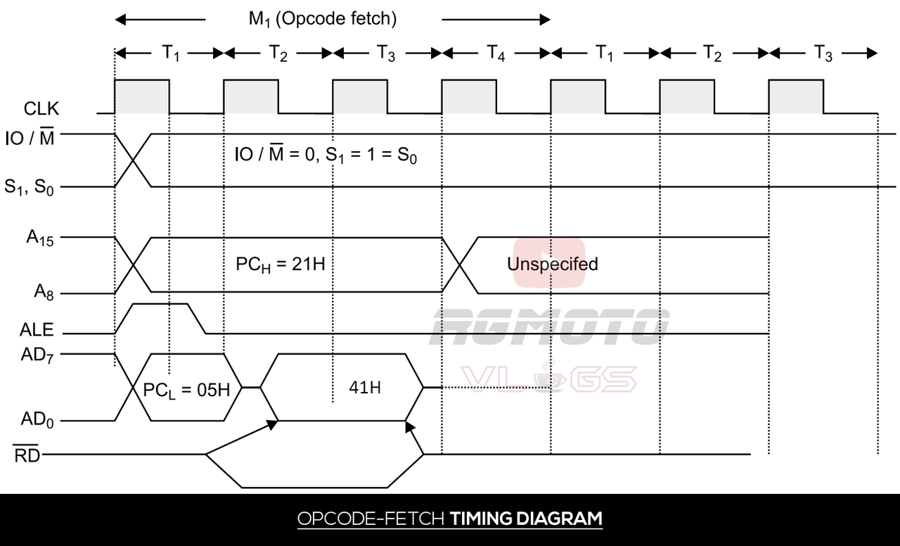
TIMING DIAGRAM OF OPCODE FETCH:
The process of opcode-fetch operation requires a minimum 4-clock cycles T1, T2, T3, and T4 and is the 1st machine cycle (M1) of every instruction.
Example: Fetch an opcode 41H stored at memory location 2105H.

For fetching an opcode, the µP must find out the memory location where it is stored. The µP fetches opcode of the instruction from the memory as per the sequence below:
• The µP resets the M(BAR) i.e.,
• The µP sends a 16-bit address. AD bus has address in the 1st clock of the 1st machine cycle, T1.
• AD7 to AD0 address is latched in the external latch when ALE = 1.
• AD bus now can carry data.
• In T2, the RD(BAR) control signal becomes reset or low for the read operation from memory.
• The memory places opcode on the AD bus
• The data is placed in the data register (DR) and then it is transferred to IR.
- EXECUTE (3 T-States):
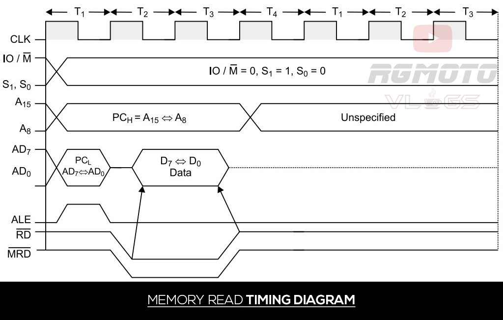
In a memory Read Cycle, the µP reads the content of a specified memory location. Afterwards, the content is placed in the Accumulator or in any register of the µP if specified so.
Example: MVI A, 05 H; Opcode is 3E and Immediate data is 05 H
The above instruction will take 2 Machine cycles i.e., M1 & M2. The 1st machine cycle (M1) will fetch and decode the opcode (3E) from the memory as specified in the above instruction. The 2nd machine cycle (M2) will read the data (05 H) from the memory.
- IO/M(BAR) goes LOW i.e., [IO/M(BAR)=0] or gets reset indicating that the address is for memory.
- S1 gets set & S0 gets reset i.e., [S1=1 & S0=0].
TIMING DIAGRAM OF READ CYCLE:

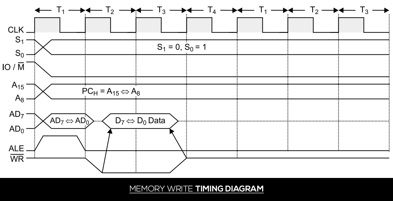
(b) Write Cycle (3 T-States): In a memory Write Cycle, the µP sends data from the Accumulator or any specified register to the memory. Here, the status signals S1 gets reset & S0 gets set i.e., [S1=0 & S0=1] for the write operation. WR(BAR) goes LOW or gets reset i.e., [WR(BAR)=0] in T2 State indicating that the write operation is to b performed.
During T2 State, the Multiplexed AD-bus is not disabled as it is to be done in case of IO/M(BAR) read operation as data is to be transmitted through this multiplexed line AD. In T3 State, WR(BAR) goes HIGH or gets set i.e., [WR(BAR)=1] because data is transmitted and there is no data transmission going on.
TIMING DIAGRAM OF WRITE CYCLE:


No comments:
Post a Comment